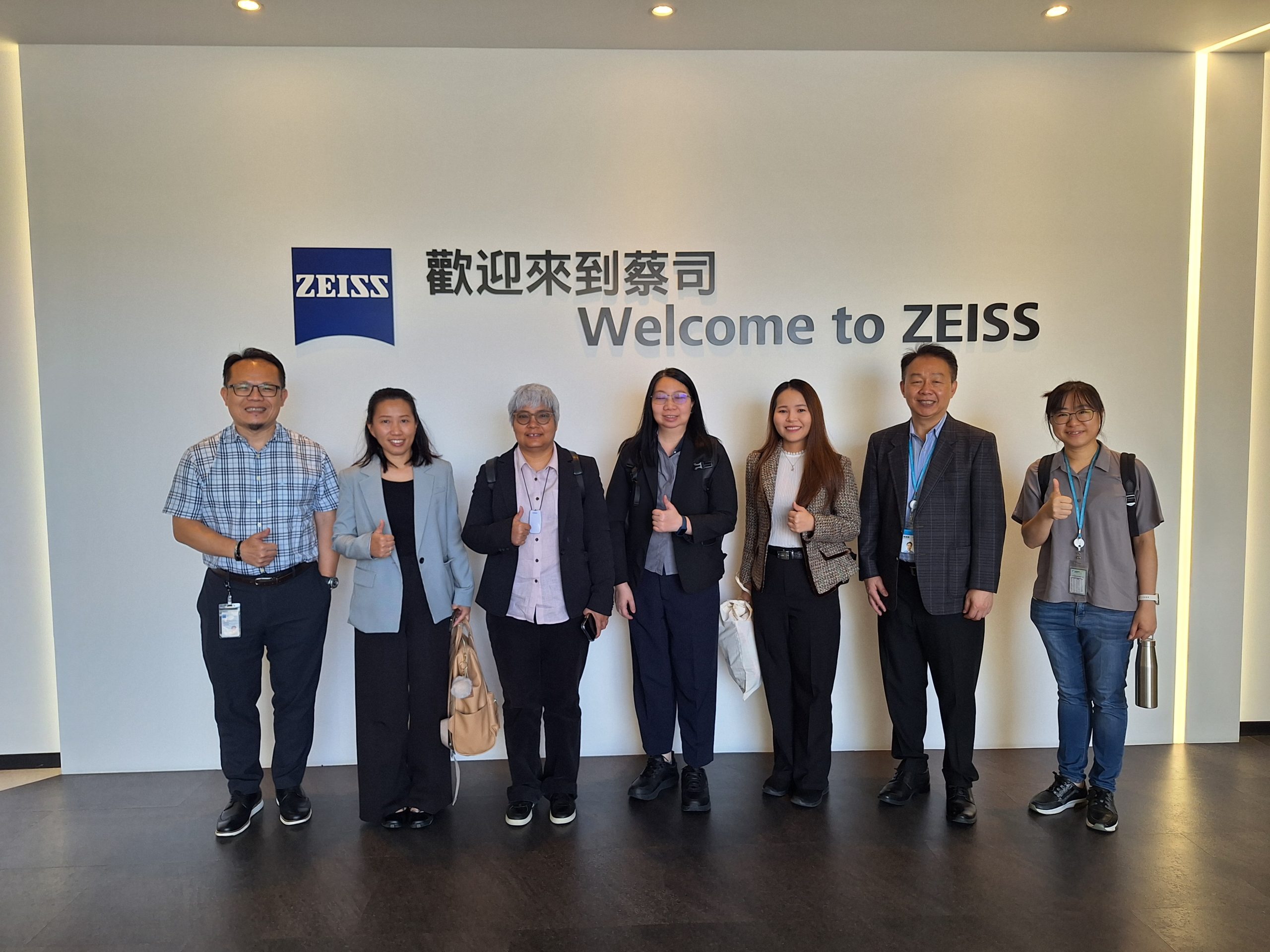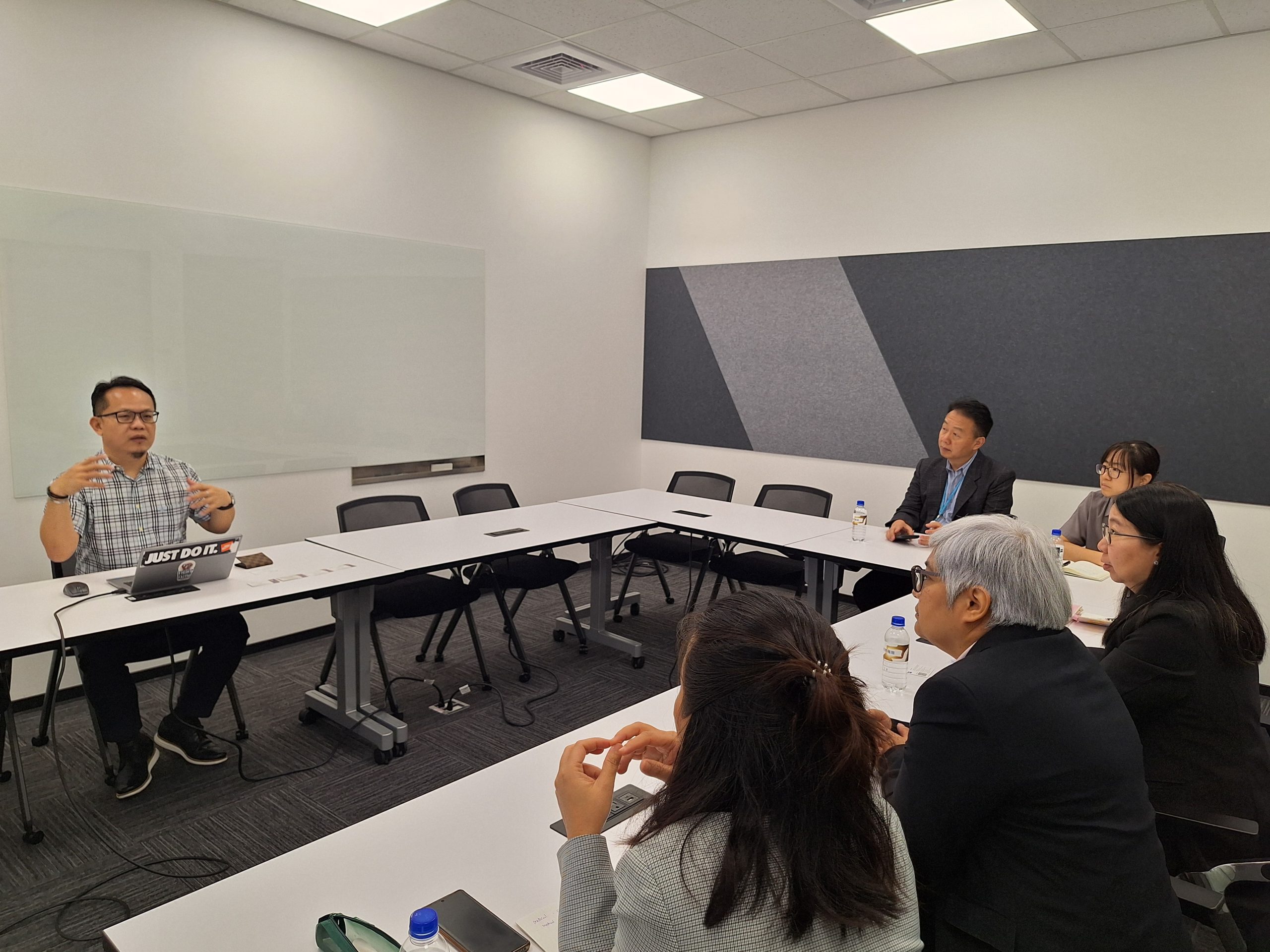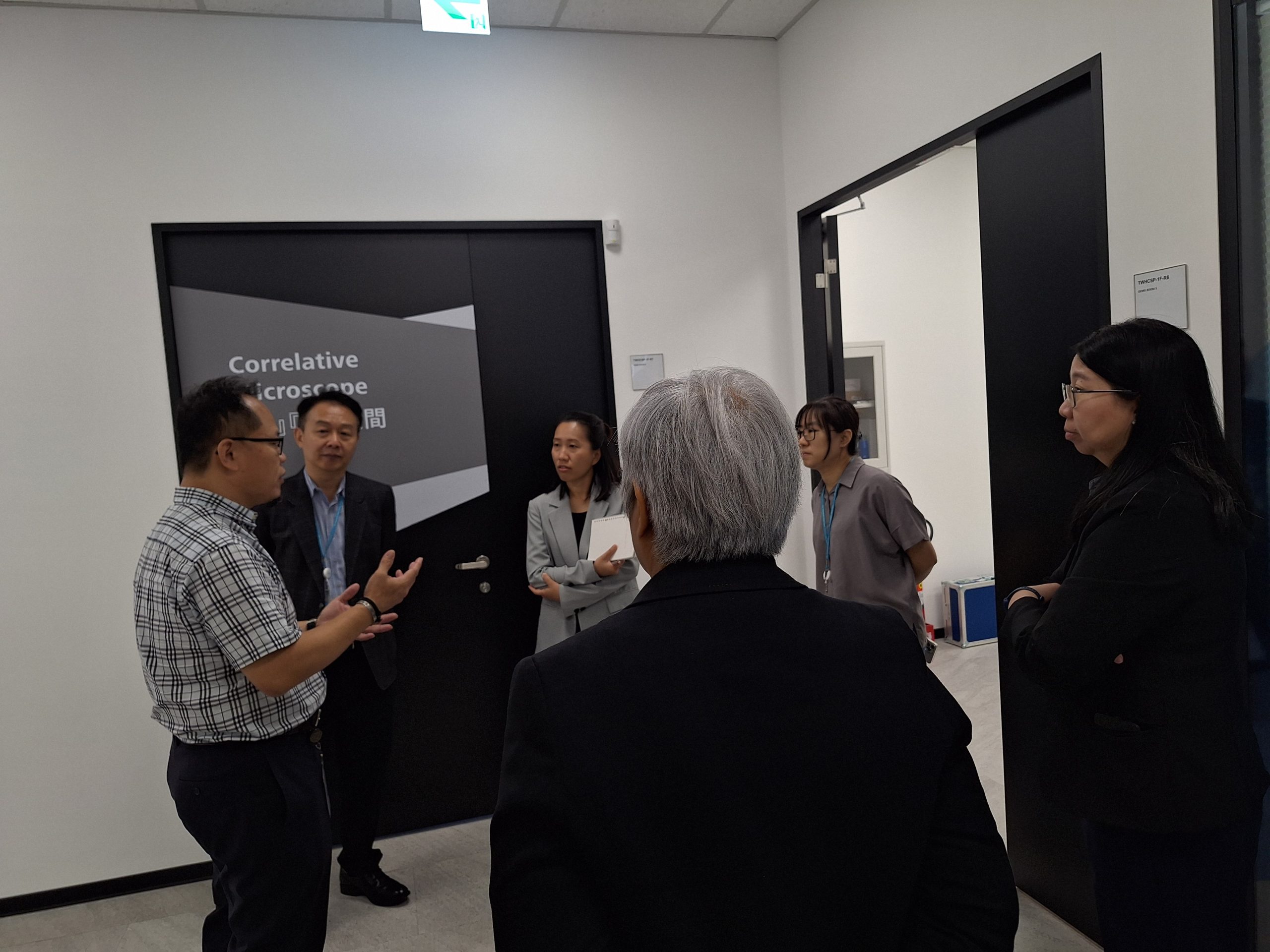
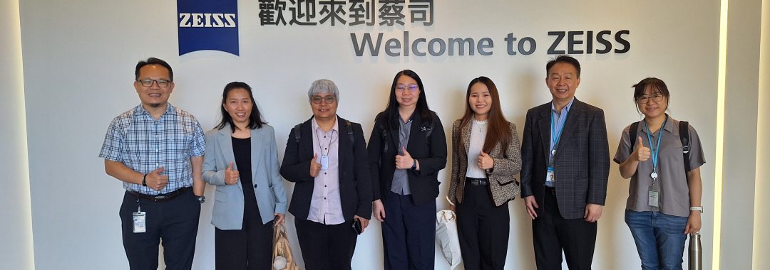
On 23 June 2025, a delegation from NIMT visited the ZEISS Innovation Center to explore cutting-edge microscopy and imaging technologies that support semiconductor and advanced material research. The visit aimed to deepen technical understanding and foster future collaboration in the field of high-resolution imaging and precision measurement.
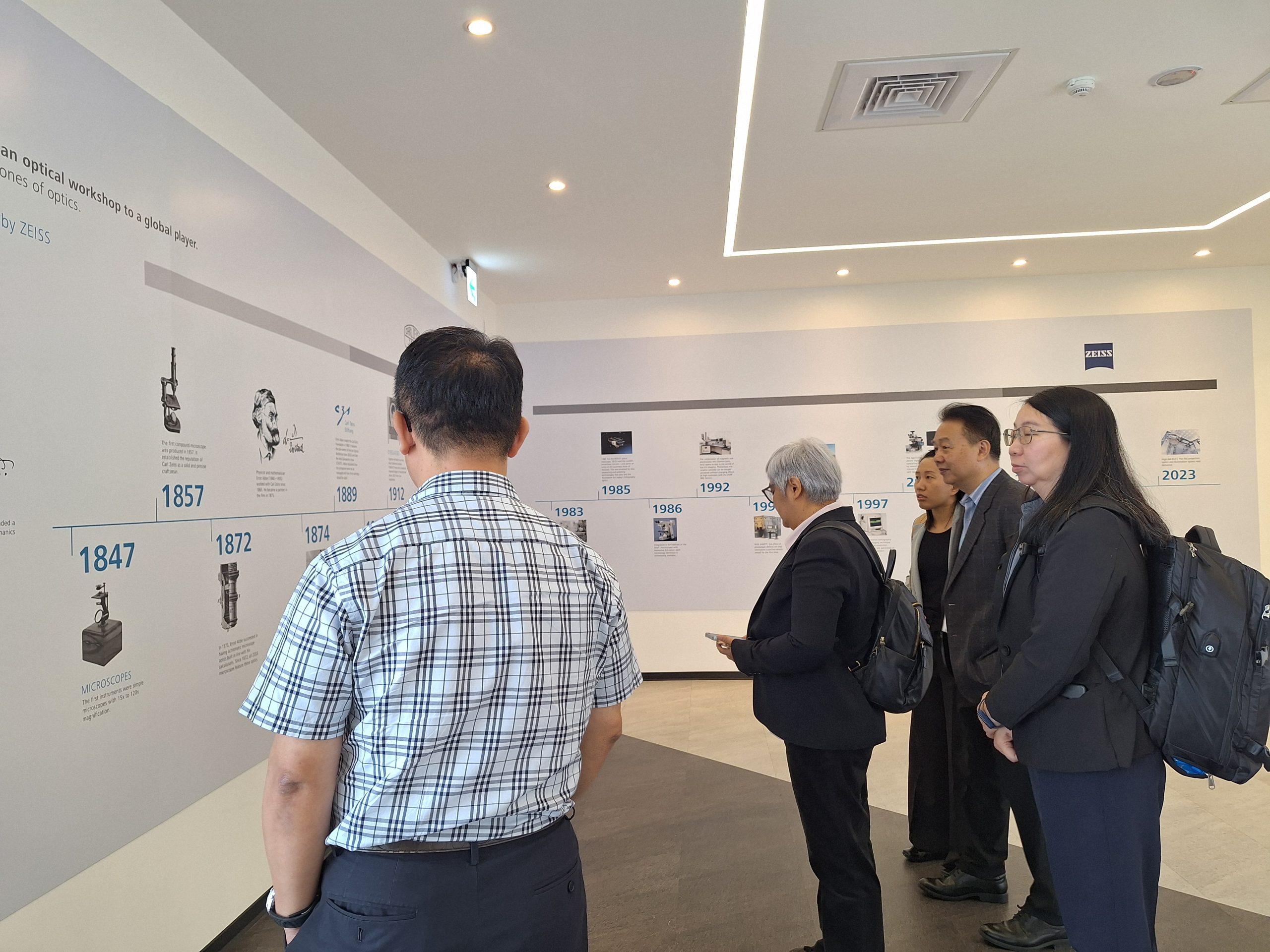
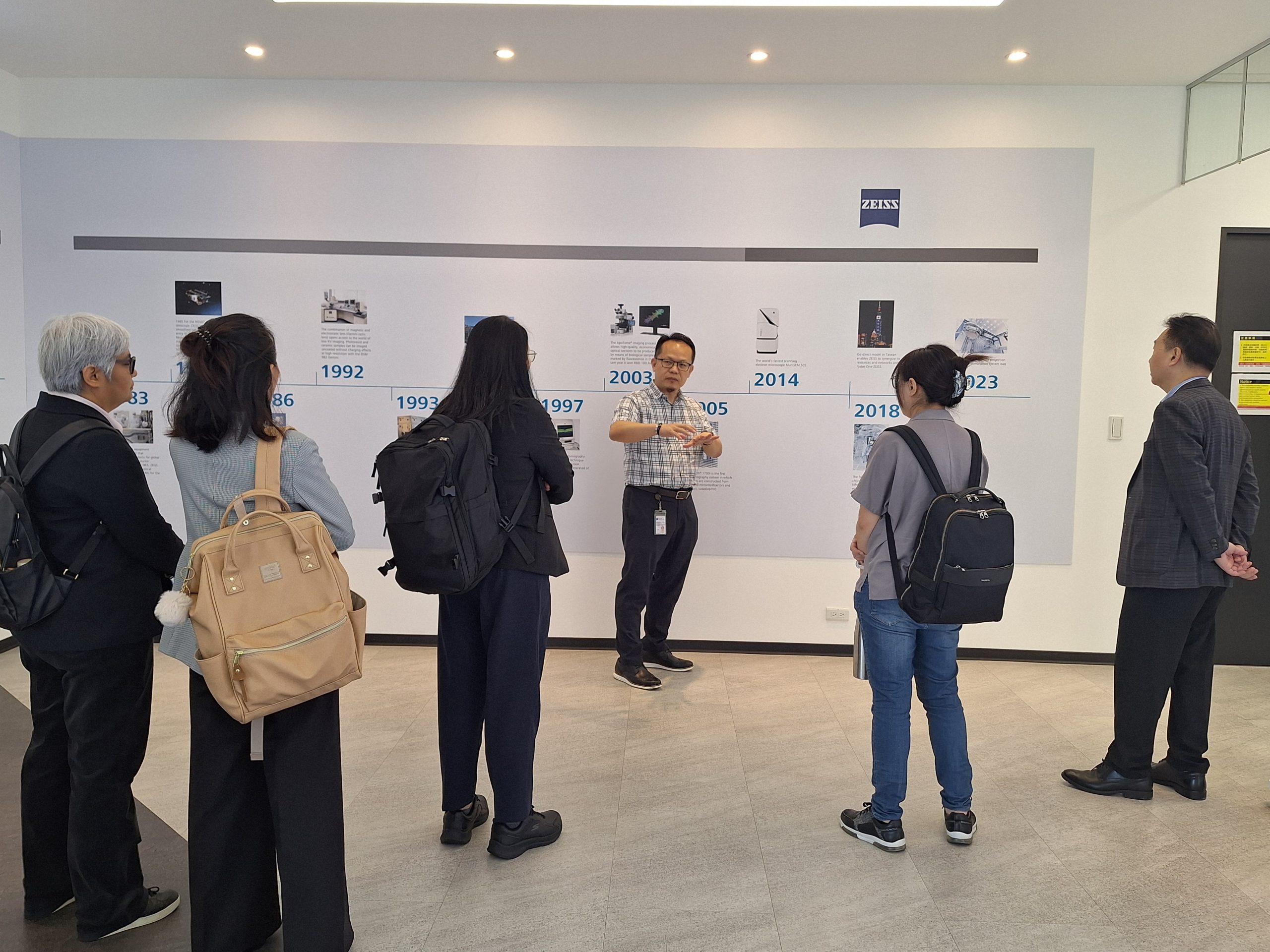
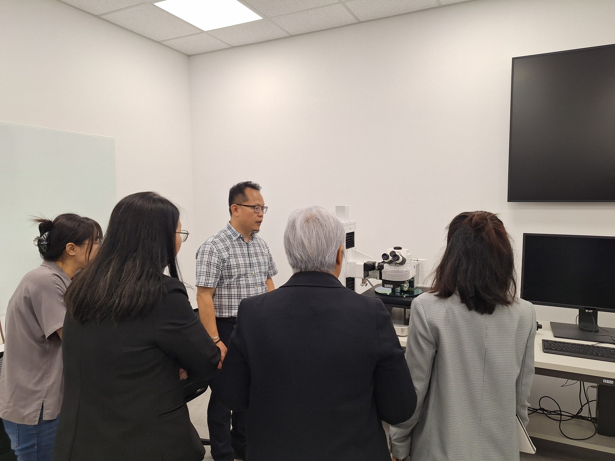
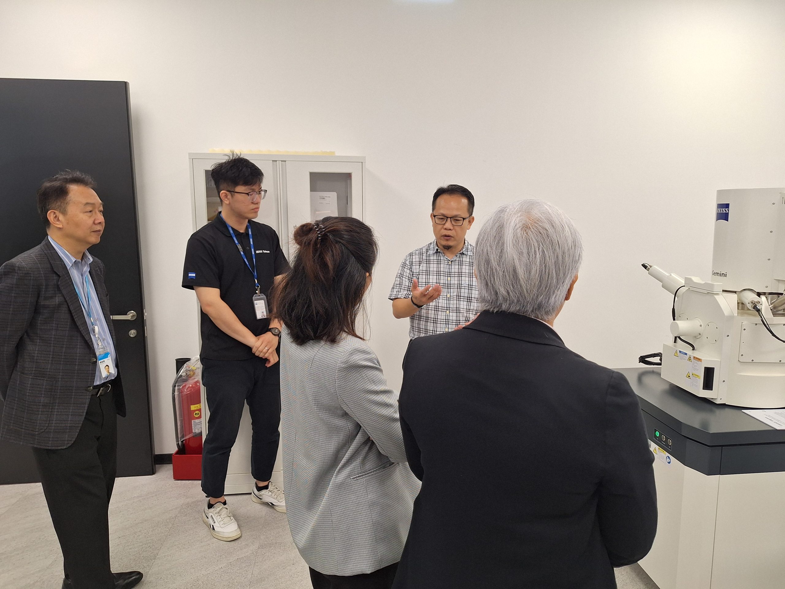
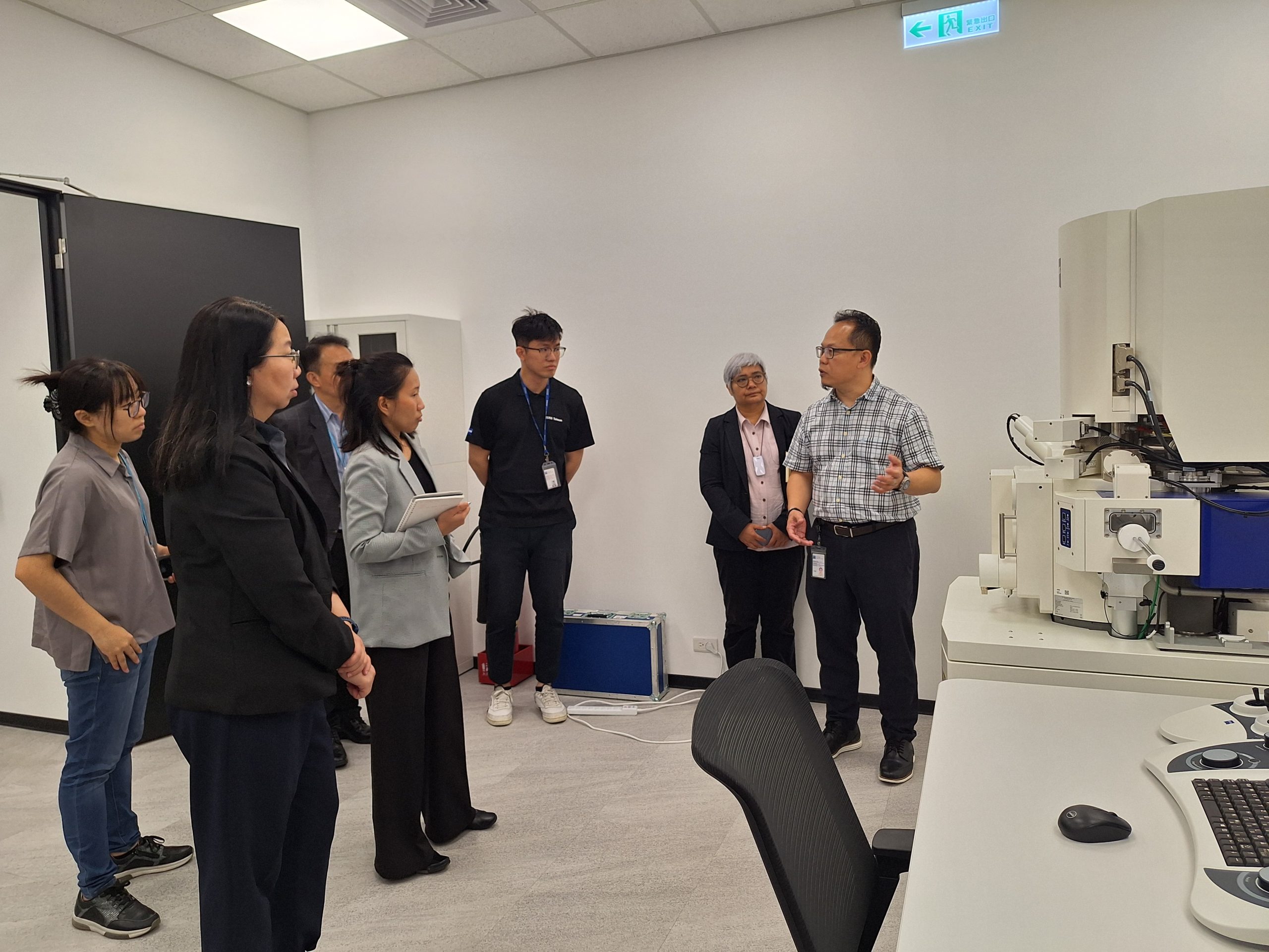
The delegation was welcomed by ZEISS Sr. Application & Business Development Manager and experts and toured several state-of-the-art laboratories, including:
– Optical Microscopy (OM) for Semiconductor – featuring advanced imaging solutions for wafer inspection and defect analysis.
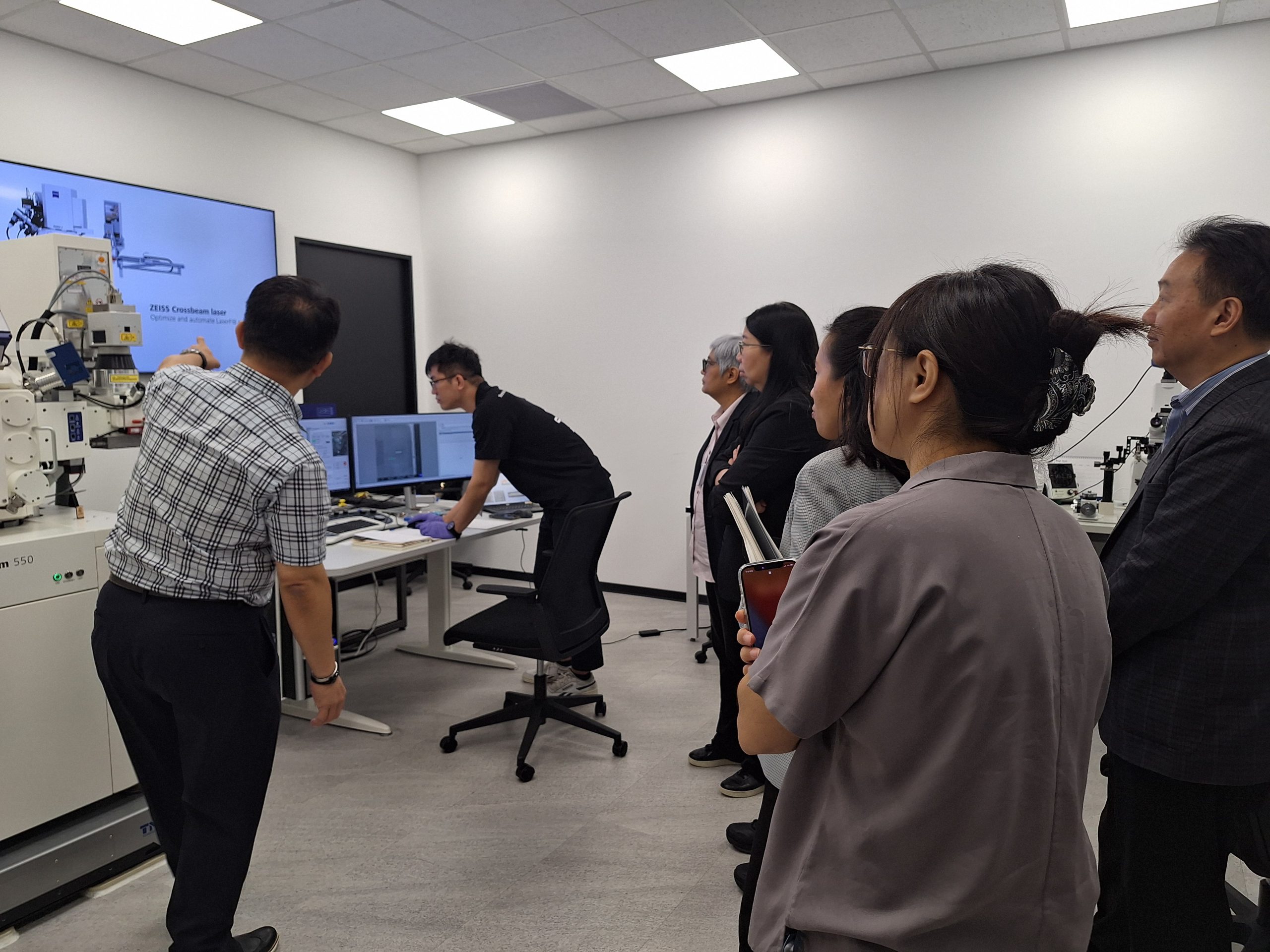
– Sigma 360 Field Emission Scanning Electron Microscope (FE-SEM) – a high-performance tool for surface morphology and nanoscale characterization.
– GeminiSEM – enabling high-resolution electron imaging with enhanced contrast and surface sensitivity.
– Femtosecond (fs) Laser Focused Ion Beam (FIB) – combining ultrafast laser ablation with precision milling for material analysis and sample preparation.
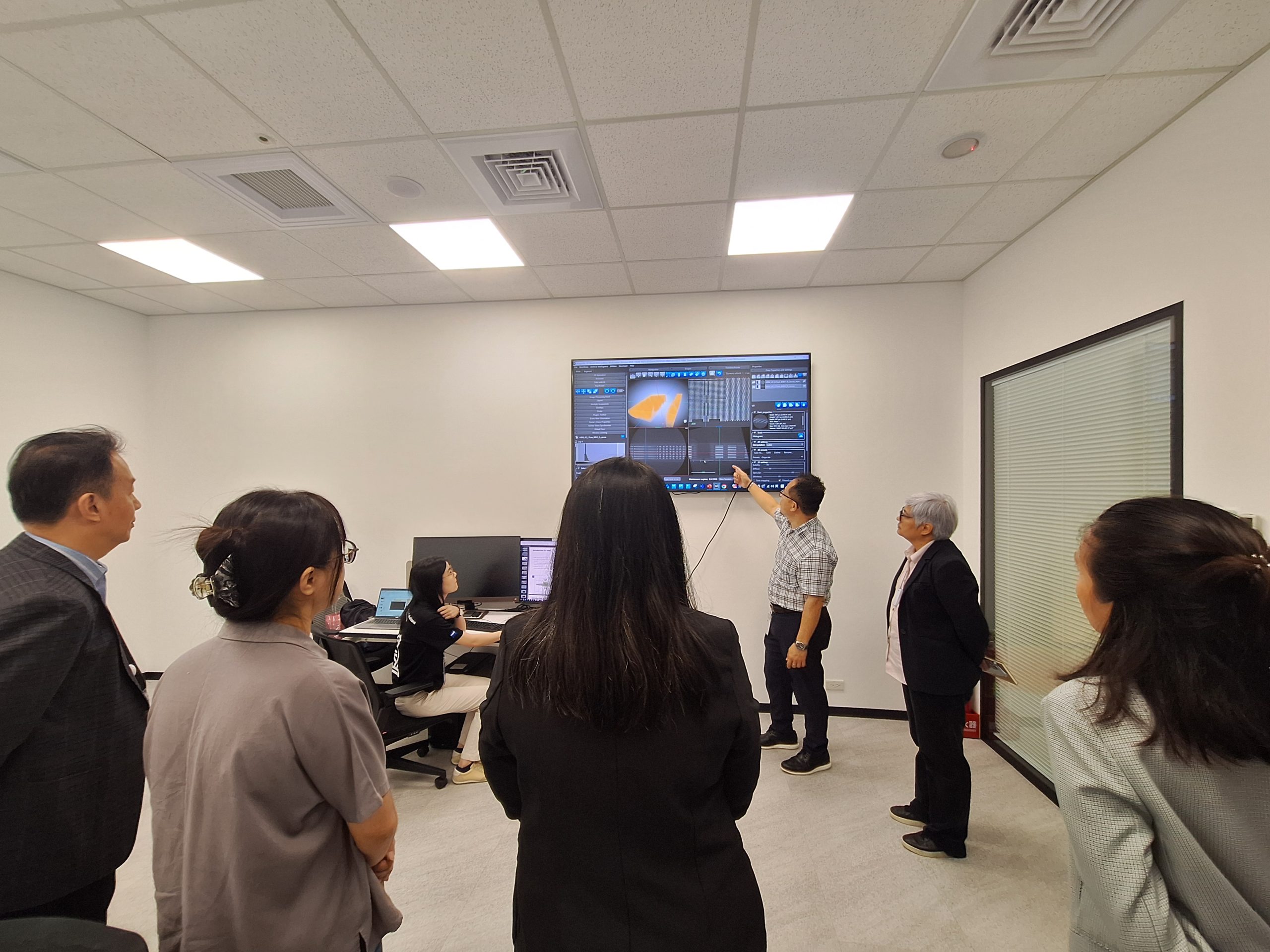
– Digital Classroom – an interactive learning platform integrating ZEISS digital tools for scientific education and collaborative research.
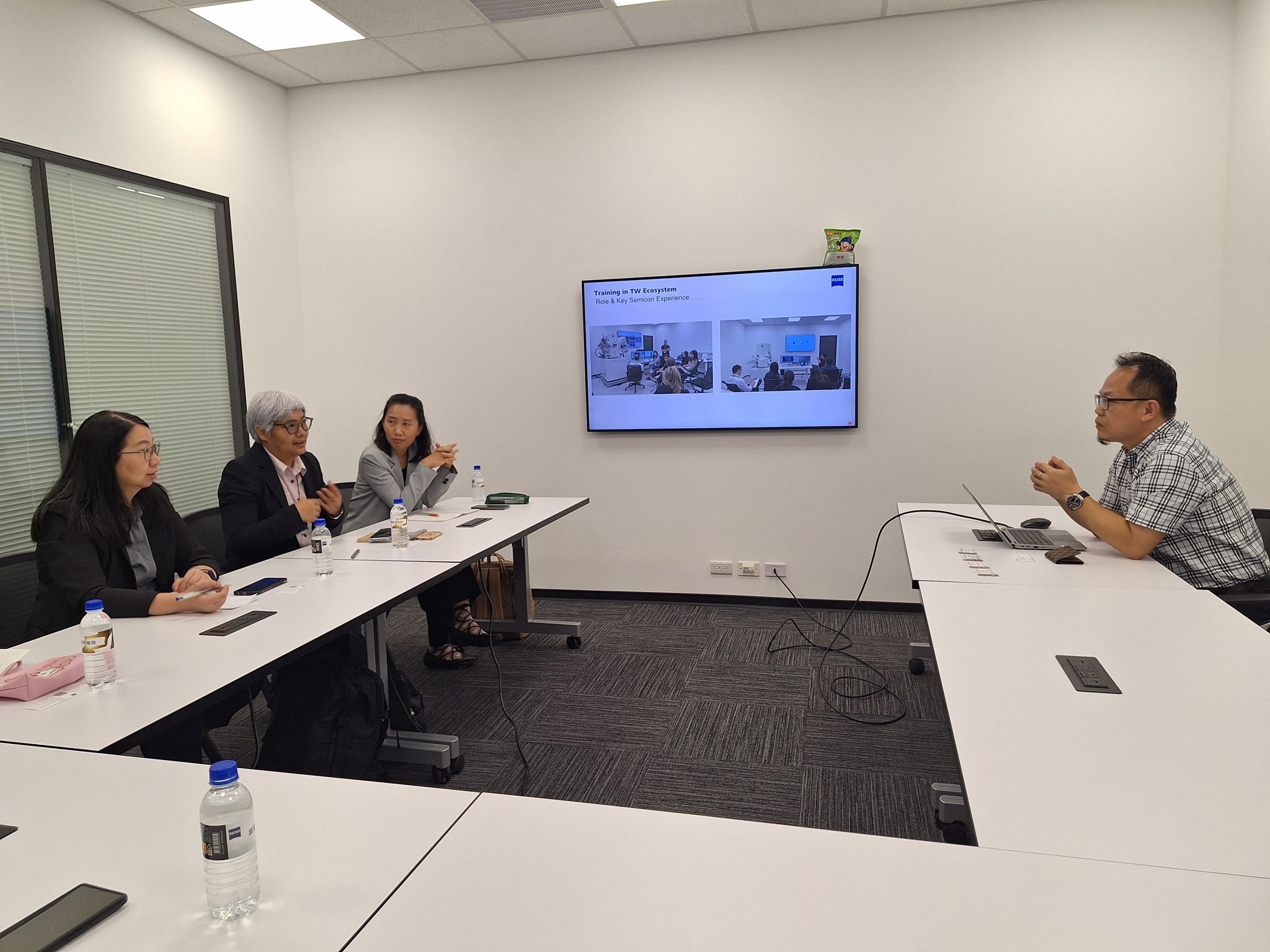
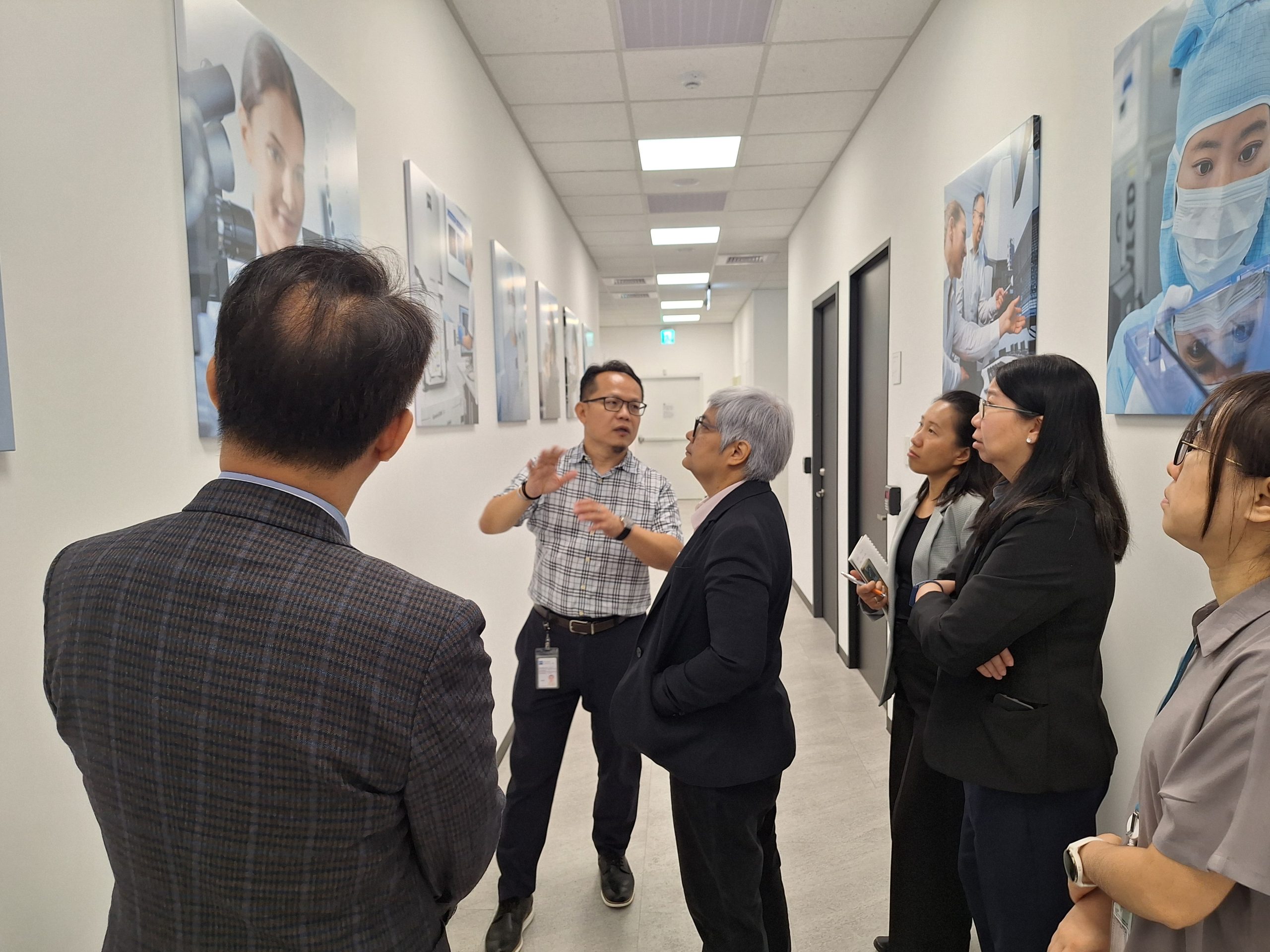
The visit concluded with an in-depth technical discussion session, where both teams exchanged views on emerging trends in metrology, imaging, and their role in supporting semiconductor innovation and quality assurance.
The engagement with ZEISS reflects NIMT’s commitment to advancing its measurement science capabilities and supporting Thailand’s high-tech sector through international collaboration and exposure to world-leading technologies.